Flat Bags on Roll is commonly used in every industry, such as electronically products, accessories,household, cosmetic, commodity, stationery, toy, fruits,vegetable and food products etc. Specially in packing of fresh fruits, fresh vegetables, meat, seafood, cakes,chocolates, candy, cookies,biscuits and so on.
The bags could be in big roll for industry and supermarket or in small or for household.
Flat Poly Bags,Flat Plastic Bags,Flat Polypropylene Bags,Flat Poly Bags On Rolls,Roll Bags,Plastic Roll Bags,Freezer Bag Rolls BILLION PLASTIC MANUFACTURING CO.,LTD, JIANGMEN , https://www.jmtshirtbag.com
Since the 1990s, China has successively introduced different types of missiles from Russia. At the same time, it has also introduced a matching missile testing system. In recent years, with the approach of the life of the missile test system, extending its service life on the basis of existing domestic technologies is an important task of the maintenance and protection department. The development of spare parts for key components of the missile test system has become an important means of prolonging the life of the system.
Based on the requirements of a type of missile test equipment, a multi-channel control circuit based on ISA bus is designed and developed. The circuit integrates 16 optically isolated input channels and 8 single-pole/double-throw (SPDT) relay output channels. Each channel inputs The output channels are equipped with indicators to identify the current status in real time. In the test system, the control circuit can distribute data signals, command signals and power signals to different circuits under the control of the ISA test bus to achieve automatic testing of missiles. The actual application results show that the developed multi-channel control circuit meets the design requirements and can completely replace the Russian circuit.
1 Introduction to the ISA Bus The ISA (Industrial Standard Architecture) bus was formed by IBM in 1984 to further expand the XT bus standard. The ISA bus standard supports 24-bit address lines and 16-bit data lines. It supports 11 interrupt IRQ3 to IRQ7, IRQ9 to IRQ12, and IRQ14 to IRQ15. It supports 7 DMA transfer channels, DRQ0 to DRQ3 and DRQ5 to DRQ7. It supports master-slave control. , I / O wait and I / O checksum and other functions. In order to maintain backward compatibility with the XT bus, the ISA bus has made special arrangements on the definition of signal functions and physical interfaces. That is, keeping the original XT bus unchanged, and adding a 36-line connection slot, which is divided into C, On both sides of D, the expanded function is designed on the signal lines on both sides of C and D. The pin is defined as follows:
1) The data bus SD7 ~ SD0SD7 ~ SD0 is an 8-bit bidirectional tri-state data bus that transfers commands, data, and status between the chip and the main interface. SD7 is the highest position.
The register select pins are SA9~SA4, SWDIP-6 (board base address 011001) and AEN#. These pins determine whether the conversion is in response to an I/O cycle. When AEN# is logic low and SA9 to SA4 match the 6-bit toggle switch exactly, a select signal is generated internally to cause the conversion to respond to an I/O cycle.
2) Address signals SA3 to SA0I/O are used as register selection signals within the FPGA chip on the conversion circuit during read and write operations.
3) Read and write signals IOR#, IOW# write operations, the conversion latches data on the rising edge of IOW#. In the read operation, when the IOR# is valid, the conversion module directly drives the 8-bit data line.
4) Interrupt signal INTR interrupt status register INTR is valid when an enable interrupt is true. There is no minimum pulse width requirement for a valid statement of INTR.
5) The IO channel ready signal IOCHRDYIOCHRDY goes low indicates that the current I/O cycle needs to be extended. In the write cycle, IOCHRDY goes high when data is latched from the ISA bus. In the read cycle, IOCHRDY goes high when the data is valid. IOCHRDY is pulled low while the register is being read or written. The IOCHRDY pin is driven with an open collector logic gate, so this signal is pulled up to a logic high level by an internal pull-up resistor.
6) When the reset signal RESETRESET signal is valid, the conversion module is triggered so that the FPGA is hard-restarted.
2 working principle shown in Figure 1, based on the ISA bus multi-channel control circuit consists of address coding, relay channels, optocoupler isolation circuit and other components. Its working principle is as follows: When the circuit works, first compare the high address of the ISA bus with the board base address set by the onboard dip switch, and the low address strobes 3 read channels and 1 write channel by address encoding. The read channel is the port 1 cache, port 2 cache, and port 3 read channel, and the write channel is the port 3 cache channel. When the IPC needs to read the feedback signal, the feedback signal is input from the interface CN2 to the 16-channel optocoupler, and the working mode is set by the resistor and jumper module. The data is written to the port 1 cache and the port 2 cache is used by the IPC to read; Each optocoupler corresponds to one LED and the current working status is displayed in real time. When the IPC needs to send a signal, the IPC writes the data to the port 3 buffer. After being driven by the relay driver, the IPC controls eight relays to be output by the DB1. At the same time, each relay corresponds to one LED and displays the current status in real time. The data written to port 3 can also be read back by reading back the address. The readback address is the same as the write address. 
3 circuit design According to the working principle can be divided into multi-channel control circuit address encoding circuit, relay control output channel circuit and optocoupler isolated input channel circuit 3 parts.
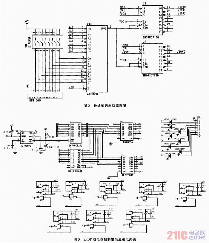
3.1 Address coding circuit Each circuit board in the test system has a unique board select address. Therefore, if a module is read or write, the board must be selected; the test system usually contains multiple circuit boards. The ISA bus cannot read and write multiple boards at the same time. Therefore, the test system requires an address coding circuit, which is located on a multi-channel control circuit. As shown in Figure 2, the address encoding circuit is composed of a pull-up resistor row, a dial switch and an encoding chip. The upper address SA2...SA9 of the ISA address bus is used as the board select address, and the board base address set by the dial switch is compared with the code chip U15. If the comparison result is the same, the gate address encoders U2 and U3 are set to the lower address SA0. SA1 is coded to obtain the read/write control signal IOR0. . IOR2, IOW0. It can be seen from the circuit diagram that the same address is used for writing and reading back the control signal of the relay channel. The board selection address encoding method is shown in Table 1. 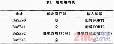
3.2SPDT relay control output circuit 8 single-pole double-throw relay control output can achieve output switch control, data read back, data stored, relay drive and work status indication function, the circuit diagram shown in Figure 3. The resistors R1, R2, the chip U16 and the capacitors C17, C18, C19 constitute the output switch control circuit; the chips U1 and U4 realize the data transfer function, data storage, and data readback functions, and the chips U9 and U10 realize the relay drive function, and the light emitting diode LED17 To LED24 for working status indication, the pull-up resistor row RP2 realizes the current limiting function for the relay driving circuit and the working state indicating circuit. The relay control output circuit is composed of the relays RLY1~RLY8 and the corresponding output filter capacitors.
As shown in Figure 3, taking one of the control channels as an example, the working principle of the SPDT relay control output circuit is as follows: the control signal is sent to the latch U4 through the data bus SD0~SD7, and is supplied to the relay driver under the control of the U4 enable signal terminal. The output of U9, U9 directly controls the pin 1 of the relay; when the control signal is low level “0â€, the relay is closed, and at the same time the LED light indicates that the channel relay is in use; when the control signal is high “1†When the relay is off and the LED is off, it indicates that the channel relay is not in use; external data is input by the interface DB1 and is output to the corresponding module through the CHA, CHB, and CHC contacts of the relay.
The working principle of data readback is as follows: The data bus SD0~SD7 first passes through the latch U4, is connected to the relay controller all the way, and the other channel is connected to the bus driver U1. When the industrial computer issues a command to read port 3, the U1 gates. The data is read back to the ISA bus.
3.316 optocoupler isolated input circuit 16 optocoupler isolated input circuit shown in Figure 4, the chip U7, U8, pull-up resistor row RP5, RP6 and light-emitting diodes LED1 ~ LED16 constitute the working status indicator circuit; chip U5, U6 And pull-up resistors RP3 and RP4 constitute data transmission and memory circuits; capacitors C1 to C16, integrated optocouplers U11 to U14, freewheeling diodes DK1 to DK16 and resistors RK1 to RK16 constitute 16 optocoupler isolated input circuits; connector JP1 And M1 to M16 form an input data state selection circuit. 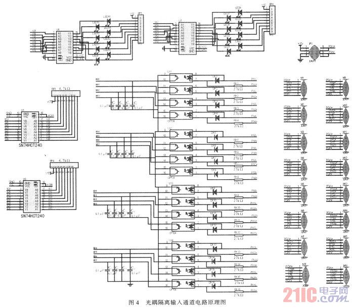
4 Experimental results The address coding circuit experimental waveforms are shown in Fig. 5. In the figure, 9, 10, and 11 indicate SA0, SA1, and /IOR, respectively, in Fig. 2, and 1 to 7 represent the chips 15 to 7 of U2 or U3 in Fig. 2. Pin. It can be seen from the experimental results that when SA0, SA1, and /IOR are all low level "0", /IOR0 is a low level "0", and /IOR0 effectively selects the corresponding module and realizes the address encoding function. 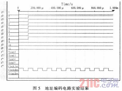

Based on ISA bus multi-channel control circuit design [Figure]
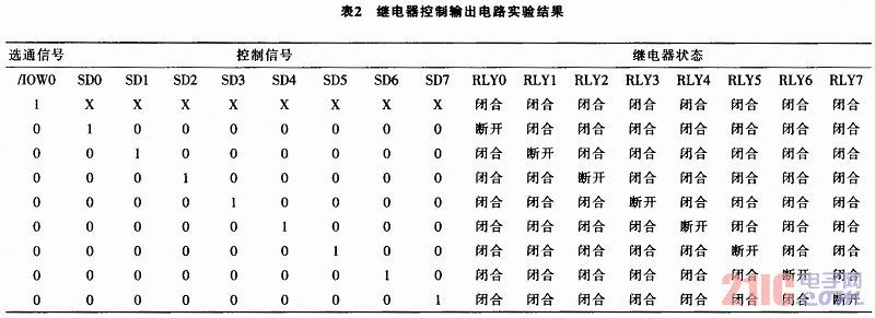
Abstract: Signal distribution is very important in the test system. A multi-channel control circuit based on ISA bus is designed according to the requirements of a missile test equipment. The circuit integrates 16 optocoupler isolated input circuits and 8 relay output circuits to complete the input and output of data signals, command signals, and power signals under the control of the ISA bus. The practical application results show that the signal distribution and transmission frequency of the multi-channel control circuit can reach 6.5 MHz, which fully meets the design requirements. The circuit is designed and standardized according to the national military standard, and has a broad application prospect in the field of testing. As shown in Figure 4, taking the first path as an example, the working principle is as follows: After IP1+ and IP1 of M1 set the operation mode of the optocoupler, the data is limited by PN1+ and PN1 of M1 and then input by the resistor RK1. The U7 pins 7 and 8 are coupled; then the pin 9 of the optocoupler U11 outputs the latch U6 pin 2 and the data pin SD0 is input via the U6 pin 18. The output data of the optocoupler is input to the 8 good pins of the driver chip U7 at the same time, and the status of the LED1 of the LED is controlled by the 12 pins of the U7 to indicate the transmitted data. If a high level "1" is input by M1, LED1 emits light; otherwise, LED1 goes out. 8-channel SPDT relay control output circuit experimental results shown in Table 2, when the strobe signal is high "1", the control signal is high impedance state "X", 8 relay state are "closed"; when the strobe signal When it is low level "0", the state of the corresponding relay changes under the action of the corresponding control signal; the design requirements are achieved. 5 Conclusions The ISA bus is the most common and commonly used test bus for test systems. The data signals, command signals, and address signals of the test system are transferred and converted under the ISA bus. Based on the requirements of a missile test system, this paper designs a multi-channel control circuit based on ISA bus. The circuit can transmit or convert signals from ISA bus through 8 SPDT relay channels and 16 optocoupler circuits. The missile test system signal distribution and transmission frequency is 6.5MHz, and the board can be normally used in the test system, so the circuit board signal distribution and transmission frequency can also reach 6.5MHz, to meet the design requirements. The board is designed according to the national military standard. After environmental experiments, electromagnetic interference experiments, and transportation experiments, the board is formally mass-produced and delivered*. The development of this board solves the difficulties of high purchase price and long period in foreign countries, and effectively improves the ability of a certain type of missile testing equipment to maintain independently. The board can also be applied to other ISA bus-based test systems, and has broad application prospects.